terça-feira, 4 de agosto de 2015

Researchers explore nanoscale structure of thin films


Tue, 08/04/2015 - 12:10pm

Laura Mgrdichian, Brookhaven National Laboratory


Simon Billinge, author on the paper and a physicist with a joint position at Brookhaven National Laboratory and Columbia Univ.'s School of Engineering and Applied Science.

Simon Billinge, author on the paper and a physicist with a joint position at Brookhaven National Laboratory and Columbia Univ.'s School of Engineering and Applied Science.The world’s newest and brightest synchrotron light source—the National Synchrotron Light Source II (NSLS-II) at the U.S. Dept. of Energy (DOE)’s Brookhaven National Laboratory—has produced one of the first publications resulting from work done during the facility's science commissioning phase.

Published July 7 in the online edition of the International Union of Crystallography Journal, the paper discusses a new way to apply a widely used local-structure analysis tool—known as atomic pair distribution function (PDF) analysis—to x-ray scattering data from thin films, quickly yielding high-quality information on the films' atomic structure. The work creates new avenues for studies of nanocrystalline thin films.

This work shows that NSLS-II—a DOE Office of Science User Facility with ultra-bright, ultra-concentrated x-ray beams—is already proving to be a game-changer in studies of thin films, which play a vital role in a large number of technologies, including computer chips and solar cells.

Thin-film challenges
In applications and during experiments, thin films (defined as having thicknesses from just a few to more than 1,000 nm, or billionths of a meter) are deposited onto a thick base, called a substrate, often made of crystalline wafers of silicon, silicon dioxide, or aluminum oxide. It is extremely difficult to study the structure of materials in this geometry because of the small amount of film material and large amount of substrate. To minimize the scattering of x-rays off the substrate, which tends to obscure the data from the tiny volume of sample, thin film x-ray studies are done using grazing incidence (GI) x-ray experiments.

In GI studies, the x-ray beam grazes the surface of the film such that it reflects off the substrate, allowing the beam to illuminate as much of the film as possible while minimizing penetration through the film into the substrate. However, the small angle of incidence makes GI studies notoriously difficult to carry out and introduces serious complexities in data analysis.

“Grazing-incidence diffraction experiments are tricky for crystalline materials, and have never successfully been done to obtain PDFs from films,” said one of the paper's authors, Simon Billinge, a physicist with a joint position at Brookhaven and Columbia Univ.'s School of Engineering and Applied Science. “The experiments are too painstaking and the data analysis is extremely challenging.”

Studying the “atomic neighborhood”
PDF provides local atomic structural information—that is, data for neighborhoods of atoms—by yielding the distances between all pairs of atoms in the sample. These distances appear as peaks in the data. In recent years, PDF has become a standard technique in structural studies of complex materials and can be used for samples that are bulk or nanoscale, amorphous or crystalline.

The approach that Billinge and his colleagues devised leverages the high fluxes of photons coming from NSLS-II, which, together with novel data reduction methods recently developed in his group, creates data suitable for PDF analysis from a thin film. Essentially, it turns the standard GI experiment on its head: the beam is simply sent through the film from the back to the front.

Eric Dooryhee, the lead scientist for the NSLS-II X-Ray Powder Diffraction (XPD) beamline, where the work was done, explained, “The first group of NSLS-II beamlines is now successfully transitioning from technical commissioning, which began back in the fall of 2014 when we first produced x-ray light, towards science commissioning, where we benchmark and test the beamline capabilities on real samples. Extracting the thin film's tiny signal from the substrate's large signal in this normal-incidence geometry is extremely technically difficult. Nonetheless, I told Simon that XPD should be up to the challenge.”

Preview of future breakthroughs
The group tested thin-film PDF (which they call tfPDF) with both crystalline and amorphous thin films, each about 360 nm thick. The collaboration includes the groups of Bo Iversen at Aarhus Univ. in Denmark and Dave Johnson from the Univ. of Oregon, who prepared the thin films.

The first sample studied was an amorphous iron-antimony film on an amorphous borosilicate substrate mounted perpendicular to the x-ray beam. In order to isolate the contribution from the film, the substrate contribution was first determined by measuring the scattering pattern from a clean substrate. The signal from the film is barely visible in the raw data on top of the large substrate contribution, but could be clearly extracted during data processing. This allowed for a reliable, low-noise PDF that can be modeled successfully to yield the quantitative atomic structure of the film.

The data led to high-quality PDFs for both amorphous and crystalline films—confirmed by comparison to control samples in a standard PDF setup. Based on the success of these first measurements, the Billinge group and the XPD team are now planning future experiments to watch the films crystallize in real time, in the beam.

“The discovery that we can get PDFs from samples in thin-film geometry so readily will revolutionize this area of science,” said Kirsten Jensen, a postdoctoral researcher in Billinge’s group at Columbia. “The experiments don’t take any specialized equipment or expertise beyond the beamline setup at XPD and are quick, opening the way to time-resolved in-situ studies of changes in film structure under processing as well as spatially resolved studies of nanostructured films in place.” 

Added Billinge, “This is an exciting new result by itself, but it only gives us a glimpse of the possibilities that NSLS-II will present as the power ramps up over the next few years. This is the tip of the iceberg of what will be possible when NSLS-II is operating at full power.”

Source: Brookhaven National Laboratory


Algae Bloom in Lake St. Clair


stclair_oli_2015209_3000

On July 28, 2015, the Operational Land Imager (OLI) on the Landsat 8 satellite captured images of algal blooms around the Great Lakes, visible as swirls of green in this image of Lake St. Clair and in western Lake Erie.

Earlier in July, NOAA scientists predicted that the 2015 season for harmful algal blooms would be severe in western Lake Erie. They suggest that algae growth in western Lake Erie could rival the blooms of 2011. Algae in this basin thrive when there is an abundance of nutrients (many from agricultural runoff) and sunlight, as well as warm water temperatures. The season runs through summer and peaks in September.

Research confirmed that in 2011, phosphorus from farm runoff combined with favorable weather and lake conditions to produce a bloom three times larger than previously observed. The researchers noted that if land management practices and climate change trends continue, the lake is likely to see more blooms like the 2011 event.

Harmful algal blooms can lead to fish kills. They also can affect the safety of water for recreation and for consumption (as was the case in Toledo, Ohio, and southeast Michigan during a 2014 bloom). As of July 30, 2015, drinking water was reported to be safe in these areas.

In April 2015, NASA and several partners announced a new multi-agency effort to develop an early warning indicator for harmful algal blooms in fresh water. The system is expected to make ocean color satellite imagery more easily available to environmental and water quality managers.

More information and annotated images: NASA Earth Observatory

Image Credit: NASA Earth Observatory images by Joshua Stevens, using Landsat data from the U.S. Geological Survey
Caption: Kathryn Hansen

Last Updated: Aug. 4, 2015

Editor: Sarah Loff

Some funny pics


pressweek-26-900x624

pressweek-36-900x601

Ugh

22 fotos incríveis de pais e filhos na mesma idade


O trabalho que vou compartilhar hoje é de origem desconhecida, porém incrivelmente interessante e com um toque de emoção.

Na galeria abaixo você vai se impressionar com a semelhança de pais e filhos, mães e filhas, avôs e netos e por aí vai! Algumas das fotos foram tiradas nas mesmas posições que seus antecessores tiraram e com a mesma idade. O resultado é simplesmente impressionante, inspire-se!

Pai e filha

22 fotos incríveis de pais e filhos na mesma idade (1)

Vó e neta

22 fotos incríveis de pais e filhos na mesma idade (2)

Mãe e filha

22 fotos incríveis de pais e filhos na mesma idade (4)

Mãe e filha e neta

22 fotos incríveis de pais e filhos na mesma idade (5)

Vó, filha e neta

22 fotos incríveis de pais e filhos na mesma idade (6)

Mãe e filha

22 fotos incríveis de pais e filhos na mesma idade (7)

Pai e filho

22 fotos incríveis de pais e filhos na mesma idade (8)

Pai e filha

22 fotos incríveis de pais e filhos na mesma idade (9)

Mãe e filha

22 fotos incríveis de pais e filhos na mesma idade (10)

Pai e filha

22 fotos incríveis de pais e filhos na mesma idade (11)

Pai e filho

22 fotos incríveis de pais e filhos na mesma idade (12)

Pai e filho

22 fotos incríveis de pais e filhos na mesma idade (13)

Pai, filho e neto

22 fotos incríveis de pais e filhos na mesma idade (14)

Mãe e filha

22 fotos incríveis de pais e filhos na mesma idade (15)

Mãe e filha

22 fotos incríveis de pais e filhos na mesma idade (16)

Pai e filho

22 fotos incríveis de pais e filhos na mesma idade (17)

Vó e neta

22 fotos incríveis de pais e filhos na mesma idade (18)

Mãe e filha

22 fotos incríveis de pais e filhos na mesma idade (19)

Pai e filha

22 fotos incríveis de pais e filhos na mesma idade (20)

Pai e filho

22 fotos incríveis de pais e filhos na mesma idade (21)

Mãe e filha

22 fotos incríveis de pais e filhos na mesma idade (22)

source:

http://www.fotoshot.com.br/22-fotos-incriveis-de-pais-e-filhos-na-mesma-idade/

GE atomic swimmer robot keeps tabs on nuclear reactors


Nuclear reactor inspector 2

The Stinger is designed to inspect nuclear reactors without the need of a human team inside the containment vessel (Credit: GE Hitachi)

One truism of nuclear reactors is that you really don't want to be next to one. Unfortunately, reactor cores need to be inspected and maintained, which means teams of workers going inside the containment vessel. It's an operation that's not only hazardous, but expensive and time consuming. In an effort to make such inspections safer, cheaper, and faster, GE Hitachi Nuclear Energy has developed the Stinger; a free-swimming, remote-controlled robot that replaces humans for cleaning and inspecting reactor vessels.

Nuclear reactors are not the easiest thing in the world to inspect. Immersed in a pool of water for coolant and to moderate the nuclear reaction, the reactor and the water vessel that contains it requires periodic cleaning and inspection to ensure that it's safe and operating efficiently. The trouble is, such inspections are expensive and surprisingly labor intensive.

Part of the problem is that special bridges need to be hauled in and installed over the pool, so workers can walk out with poles tipped with tools and instruments to do their job. This operation is not only burdensome, but it also exposes the team to radiation, which the industry obviously tries to avoid, and interrupts the on-going operations to remove and replace spent fuel rods.

The GE Hitachi Stinger is designed to simplify the whole inspection task by replacing the team and the bridge with a free-swimming robot that looks a bit like a gigantic mechanical seahorse. Instead of using a rail or a track, the robot swims about using an advanced camera and remote positioning technology while being controlled by an operator in a tent away from the radiation area. This not only removes the need for a bridge, but also allows refueling operations to continue uninterrupted.

"Stinger performs inspections of welds within nuclear reactors. It remotely operated and swims to these welds within this highly irradiated area," said Jerry Dolan, Senior Tooling Manager at GE in an interview with Gizmag. "Stinger uses a hydrolaser to blast welds with water before it shoots HD video of the weld. This video is then beamed near real-time to Nuclear Regulatory Commission-approved inspectors at our global Center of Excellence in Wilmington, NC, where they are analyzed.

"Stinger literally replaces eight people standing on the bridge of the reactor lowering cameras and brushes with ropes and pulleys. It is much faster and more accurate than previous methods while also significantly reducing radiation dose."

Dolan went on to explain that the robot uses multiple thrusters to navigate, and depth, pitch, and roll sensors stabilize and position itself.

In a separate interview, John Lizzi, Manager of the Distributed Intelligent Systems Laboratory at GE Global Research, sites the Stinger as one example of the company's service robotics strategy. The robot been in operation for 1½ to 2 years, and in the future it may be upgraded to carry out maintenance and repair operations as well as inspections.

Source: GE Hitachi

Innovations from the wild world of optics and photonics


Princeton research team explores ways of communicating and processing signals with light waves

image showing a silicon photonic platform

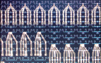
A silicon photonics platform connecting excitable lasers to form a photonic neural network.

July 31, 2015

Traditional computers manipulate electrons to turn our keystrokes and Google searches into meaningful actions. But as components of the computer processor shrink to only a few atoms across, those same electrons become unpredictable and our ability to shuttle them across long and short distances diminishes.

With support from the National Science Foundation (NSF), the Lightwave Communications Laboratory at Princeton University, led by Paul Prucnal, seeks to understand, build, and design the next generation of communication systems that process information far faster than today's devices using photonics, or the manipulation of light.

The field of photonics began, roughly, with the invention of the laser in the late 1950s and found widespread applications in the 1990s with the explosive growth of the Internet.

Photonics not only made high-speed long-distance data transmission via fiber optic cables feasible and affordable, it has also enabled advances in laser manufacturing, chemical sensing, medical diagnostics, display technologies and many other fields.

But scientists are betting that not all of light's secret abilities have been discovered yet.

In his lab at Princeton, Prucnal and his team have been experimenting with a variety of optics and photonics-based applications, creating systems to carry hidden messages, detect malicious cyber-attacks and improve the quality and capacity of wireless communications using light.

They are even exploring whether it may be possible to create a network of photonic "neurons" to perform functions our brain does well--like pattern recognition--but significantly faster. Through partnership with industry, their innovations are moving quickly from the lab to the factory.

Coping with billions of devices

Currently, there are more mobile communication devices than humans on the planet, and this proliferation is expected to continue. However, the radio bandwidth on which wireless communications depend is a limited resource.

As more and more devices compete for bandwidth, we can expect more bottlenecks and more interference from nearby competing antennas, said Matthew Chang, a Ph.D. student in Prucnal's lab. To handle the constant growth in demand for capacity and bandwidth, optical solutions are needed.

"With a frequency 1 million times bigger than radio waves, optics sees the entire current radio-wave spectrum as practically a single frequency," Chang said. "In terms of its ability to provide the bandwidth for a growing army of mobile phones, we say it's future proof."

In the near term, the lab is working on technologies that harness optical signal processing to improve the efficiency of the cell towers and mobile antennas already in place.

One such technology the lab developed is called photonic beamforming. It involves encoding wireless signals on light waves to allow antennas to selectively detect signals from a desired spatial direction, operating with precision and over bandwidths that exceed what is possible with electronics.

The phenomenon is akin to "the cocktail party effect," where one is able to tune in to the frequency and direction of a friend's voice in a crowded room.

The human brain is adept at de-noising signals, Chang explained. "We know what direction the voice is coming from and can train our ears to sense in that direction."

We also know what a friend's voice sounds like and can even read lips if we need to, he said. Radio antennas can't do that.

"We want to design processors that give radio antennas the ability to sense a signal, lock on its spatial direction, and follow it to the source," Chang said.

The technology that the team developed utilizes an array of antennas coupled to an adaptive processor to filter signals in both space and frequency. The technology allows the processor to steer the beam of radio waves while rejecting interfering directional noise sources.

Their techniques can even apply algorithms that let the antenna system adapt to rapidly changing environments in order to track fast moving targets or rapidly switch between a wide-angle search and detailed inspection.

Not surprisingly, many of the group's technologies are current of interest to the military. However, they imagine that one day every cell phone will contain a beamforming chip to better manage wireless inputs and outputs, the way many of today's phones contain a small component to switch between different wireless channels.

Working with partners L3 Telemetry East and Bascom Hunter Technologies, which Prucnal helped found, the researchers are transferring the beamforming technology from the laboratory to the marketplace.

Bascom Hunter received Phase 1 Small Business Innovation Research (SBIR) support from NSF in 2013 and 2015 to adapt their technologies for public safety radio networks and to improve the intermediate links between the core networks. They hope to see the technology improving the performance of cellphone towers and military applications within one or two years.

More importantly, as data rates climb exponentially, the group sees optics and photonics as a way to provide gigabit or faster Internet to everyone, without the use of optical fiber.

"The current processing of radio signals is akin to trying to sense and map the changing surface of the ocean by slowly sucking water through a single straw," said Prucnal. "Photonic processing makes it possible to process radio signals with greater precision and parallelism, and with greater speed, than electronics."

Building a laser-fast brain

If light-encoded Wi-Fi signals sounds far-out, another of the projects in Prucnal's lab is truly at the distant frontiers of research: the photonic neuron.

The project came out of conversations between Prucnal and David Rosenbluth, a neuroscientist at Lockheed Martin, with which the lab collaborates. Prucnal noticed that the differential equations that describe the behavior of neurons have the same forms as the equations for lasers.

Furthermore, in biological neurons, each has an internal voltage. If that voltage reaches a certain point, the neuron emits a spike, signaling the neurons to which it is connected.

Likewise, a laser gets pumped with current, exciting more electrons from one state to another; at a certain point, the laser reaches its threshold and outputs an optical spike.

The dynamics, they noted, were astonishingly similar, but lasers have the potential to perform the same action a billion times faster than the chemical signaling in the brain.

This led the researchers to wonder if it was possible to design a synthetic system made of optical and photonic materials that could perform some of the functions of a physiological neuron.

After developing a single photonic neuron in 2009, the research team has been working to build sophisticated, ultrafast signal processing circuits that mimic the visual, auditory, and motor functions found in biological organisms.

Their initial implementation was inspired by the crayfish tailflip response--a natural wonder of high-speed sensing.

Crayfish have a neuronal circuit in their brain that is networked in such a way that, if it senses danger, a specific set of neurons fire simultaneously, causing the creature to flip its tail to swim away with amazing speed.

With this biological model in mind, Prucnal and his team designed a system that uses several excitable lasers, pre-loaded in such a way that if a particular signal comes in, the lasers recognize the specific pattern and fire a spike together.

In the future, the researchers say such a device could be capable of making nearly instantaneous calculations in life-or-death situations, such as deciding whether to eject a fighter pilot from a jet.

"When thousands of photonic neurons are networked together and working in unison, we believe we can build a processor that can sense patterns and cues with an almost human-like quality, but a billion times faster," said Bhavin Shastri, a post-doctoral fellow at Princeton working on the project.

For example, the team imagines being able to peer into all the wireless signals around you, lock onto one of interest, and take action on it--all in an instant as the signal zooms across your antenna.

The lab's research was featured on the cover of the IEEE Photonics Society Newsletter in June 2014; and in November 2014, the group published an article in IEEE's Journal of Lightwave Technology describing how to scale the signal-processing platform to large numbers of neurons.

By finding new ways to encode and process light and by applying these methods to existing and brand new applications, Prucnal's group is helping to solve the looming bandwidth shortage while imagining entirely new capabilities for photonic systems.

"With all the information that can be obtained using photonic processing of the radio image, we could track signals coming from all directions and all frequencies, separating multiple signals of interest from multiple interferers, quickly finding holes in the radio spectrum available for transmission, and mapping out spatial features of the radio environment in real-time," Prucnal said. "This vision is not only exciting, but will be necessary as the use of wireless communications proliferates in the future."

--
Aaron Dubrow, NSF (703) 292-4489 adubrow@nsf.gov

Investigators
Paul Prucnal

Related Institutions/Organizations
Princeton University

Locations
Princeton , New Jersey

Related Programs
Networking Technology and System
Enhancing Access to the Radio Spectrum

Related Awards
#1217435 NeTS: Small: Collaborative Research: OSTARA: An Optically-based Simultaneous Transmit and Receive Architecture for Enhancing Wireless Communications
#1247298 EARS: Collaborative Research: Big Bandwidth: Finding Anomalous Needles in the Spectrum Haystack

Years Research Conducted
2012 - 2015

Total Grants
$450,000

Related Websites
International Year of Light: http://www.light2015.org/Home.html
Lightwave Communication Laboratory: http://ee.princeton.edu/research/prucnal/node?destination=node

source : http://www.nsf.gov/discoveries/disc_summ.jsp?cntn_id=135842&WT.mc_id=USNSF_51&WT.mc_ev=click

World's highest-performance single-molecule diode created


The creation of a single-molecule diode that is 50 times more efficient than anything produced before may help pave the way for much more practical molecular electronic components

The creation of a single-molecule diode that is 50 times more efficient than anything produced before may help pave the way for much more practical molecular electronic components (Credit: Latha Venkataraman/Columbia University)

As electronics miniaturization heads towards a theoretical physical limit in the tens of nanometers, new methods of manufacturing are required to produce transistors, diodes, and other fundamental electronic components. In this vein, a new range of molecule-sized devices have been created in the laboratory, though with varying results in terms of efficiency and practicality. Now a group of researchers from Berkeley Lab and Columbia University claims to have created the highest-performing, single-molecule diode ever made, which is said to be 50 times better in performance and efficiency than anything previously produced.

Ordinary diodes are usually constructed from silicon with a p-n (positive-negative) junction created at the point of contact between a positively "doped" semiconductor (that is, one that has had its electrical properties altered with additives) and a negatively doped one. Flanked by connecting electrodes (an anode on one side and a cathode on the other), the most common function of such a diode is to permit electric current to flow in one direction only, whilst blocking current from flowing in the reverse direction. As such, a diode used in this way can be seen as a type of flow-control valve that is either "on" or "off". Technically, this one-way behavior is known as rectification as it can, for example, be used to rectify alternating current to direct current, and so these types of diodes are known as rectifiers.

This on/off – asymmetric – behavior in the nascent field of molecule-sized electronics, on the other hand, is usually achieved by the creation of molecules that chemically emulate the p-n junction. However, these synthesized molecular junctions have generally resulted in poor forward current flow capabilities and inefficient or patchy rectification. This is where the Columbia university scientists claim to have made significant improvements with their new single-molecule diode.

Diagram of the molecular junction that functions as a diode, allowing current to flow in one direction only

"Using a single symmetric molecule, an ionic solution and two gold electrodes of dramatically different exposed surface areas, we were able to create a diode that resulted in a rectification ratio, the ratio of forward to reverse current at fixed voltage, in excess of 200, which is a record for single-molecule devices," said Jeffrey Neaton, director of the Berkeley Lab’s Molecular Foundry and professor at the University of California Berkeley. "The asymmetry necessary for diode behavior originates with the different exposed electrode areas and the ionic solution. This leads to different electrostatic environments surrounding the two electrodes and superlative single-molecule device behavior."

First mooted in 1974 by Mark Ratner and Arieh Aviram, an asymmetric molecule that could act as a rectifier has been a long sought after goal, particularly as diodes form the basis of many microminiature electronic devices. Since then, a range of devices have been constructed, including single molecule diodes and transistors. Operating at this nanoscale, though, such devices may emulate their macro counterparts, but that behavior is merely a simulation; at such scales the electronic operation of these devices is governed more by quantum influences.

"Electron flow at molecular length-scales is dominated by quantum tunneling," said professor "The efficiency of the tunneling process depends intimately on the degree of alignment of the molecule’s discrete energy levels with the electrode’s continuous spectrum. In a molecular rectifier, this alignment is enhanced for positive voltage, leading to an increase in tunneling, and is reduced for negative voltage. At the Molecular Foundry we developed an approach to accurately compute energy-level alignment and tunneling probability in single-molecule junctions. This method allowed myself and Zhenfei Liu to understand the diode behavior quantitatively."

Zhenfei Liu – a postdoctoral fellow at Berkeley Lab – and professor Neaton worked with Latha Venkataraman and Luis Campos from Columbia University to create their high-performance rectifier diode using junctions prepared from symmetric molecules attached to gold electrodes. To achieve the necessary asymmetric properties required to operate as a diode, the researchers then altered the surface area of the electrodes as they were exposed to an ionic solution. As a result, a positive voltage increased the current significantly, whilst a negative voltage reduced current flow in an equally significant manner.

"The ionic solution, combined with the asymmetry in electrode areas, allows us to control the junction’s electrostatic environment simply by changing the bias polarity," said professor Neaton. "In addition to breaking symmetry, double layers formed by ionic solution also generate dipole differences at the two electrodes, which is the underlying reason behind the asymmetric shift of molecular resonance. The Columbia group’s experiments showed that with the same molecule and electrode setup, a non-ionic solution yields no rectification at all."

The combined Berkeley Lab-Columbia University research team is convinced that the way they have managed to produce a single-molecule diode sets the benchmark for future nonlinear nanoscale device tuning and development, with applications above and beyond just junctions of single-molecule components.

"We expect the understanding gained from this work to be applicable to ionic liquid gating in other contexts, and mechanisms to be generalized to devices fabricated from two-dimensional materials," said professor Neaton. "Beyond devices, these tiny molecular circuits are petri dishes for revealing and designing new routes to charge and energy flow at the nanoscale. What is exciting to me about this field is its multidisciplinary nature – the need for both physics and chemistry – and the strong beneficial coupling between experiment and theory. With the increasing level of experimental control at the single-molecule level, and improvements in theoretical understanding and computational speed and accuracy, we’re just at the tip of the iceberg with what we can understand and control at these small length scales."

The results of this research were recently published in the journal Nature Nanotechnology.

Source: Berkeley Lab

Three-protein biomarker raises possibility of a urine test for pancreatic cancer


Scientists have uncovered a new biomarker that suggests a urine test for pancreatic cancer could one day become a reality

Scientists have uncovered a new biomarker that suggests a urine test for pancreatic cancer could one day become a reality (Credit: Pancreatic Cancer Research Fund)

With a lack of clear symptoms even when the disease is well progressed, more than 80 percent of pancreatic cancer diagnoses come after the cancer has already spread. This has led some researchers to look beyond blood to urine testing, which is a less complex fluid. Among those is a team at the Queen Mary University of London, which has uncovered a three-protein biomarker in the urine of pancreatic cancer sufferers, suggesting a less invasive, early stage test may be on the way.

At just three percent, the five-year survival rate for pancreatic cancer is lower than any form of common cancer. Because it is difficult to detect, sufferers are often diagnosed after it has already spread which rules out surgical removal of the tumor, the only current method of treatment. Adding to the complexity are the difficulties in distinguishing between pancreatic cancer and the inflammatory condition known as chronic pancreatitis. But the Queen Mary researchers say they have made progress in addressing both problems.

The scientists gathered a total of 488 urine samples. 192 came from patients with pancreatic cancer, 92 from those with chronic pancreatitis, 87 from healthy volunteers and another 117 from patients with benign and malignant liver and gall bladder conditions. They tallied around 1,500 proteins in the urine samples, but zeroed in on three in particular for a closer look: LYVE1, REG1A and TFF1.

The pancreatic cancer sufferers had higher levels of all three proteins than the healthy patients. And in a discovery that could help separate them from those with chronic pancreatitis, the latter group displayed significantly lower levels of these proteins. The researchers say that the combined three-protein signature can help detect stage one and two pancreatic cancer with more than 90 percent accuracy. Stage two detection carries a survival rate of 20 percent, while stage one can see survival rates of up to 60 percent.

"This is a biomarker panel with good specificity and sensitivity and we’re hopeful that a simple, inexpensive test can be developed and be in clinical use within the next few years," says lead researcher Dr Tatjana Crnogorac-Jurcevic.

From here, the team aims to carry out further tests on people from high risk groups which includes those with obesity, a family history of pancreatic cancer, heavy smokers and people over 50 with new-onset diabetes. They are also hopeful of collecting ongoing samples from volunteers over the next five to ten years.

Studying samples of those who went on to develop pancreatic cancer could allow them to establish if the three-protein biomarker is present during the latency period. This refers to the time after the genetic changes take place that cause the cancer develop and before the clinical presentation.

The research was published in the journal Clinical Cancer Research.

Source: Queen Mary University of London

Bevel brings another dimension to smartphone photography


Bevel is a 3D photography attachemnt that works with both iOS and Android devices

Bevel is a 3D photography attachemnt that works with both iOS and Android devices

Image Gallery (7 images)

Sticking with what it knows, Toronto-based Matter and Form has created Bevel, an accessory that turns smartphones and tablet into 3D cameras. Unlike the 3D Scanner the team released last year, Bevel isn't specifically intended for creating detailed 3D models of objects for 3D printing or animating, but for capturing everyday events that can then be shared in 3D.

Bevel connects to iOS or Android devices via the headphone jack and allows users to capture three-dimensional images without much more effort than taking your standard photograph. The device packs an eye-safe laser which the photographer pans over the subject to capture depth information, while the mobile device's camera takes a photo as normal. The optimum subject distance is currently around 1 m (3.3 ft), the the team is looking to bring the capability to capture buildings and even entire cities in a future release.

The resulting image can then be viewed within the Bevel app and the company’s app, Cashew, which allow users to share 3D photos in places like Twitter, Facebook, Tumblr, and Pinterest. Images can be rotated within the apps to can get just the right angle and can also be turned into animated GIFs or saved to be used later in an animation or 3D printing project –although the team says it is still ironing out the details on exactly how 3D printing compatibility will work.

The choice of device to pair with Bevel will make a difference to image quality, with Matter and Form recommending a device with an accelerometer and a gyroscope, and Kit-Kat or higher for Android devices and iOS or higher for iOS devices. Bevel is powered by its own rechargeable battery so won't drain the mobile device it's connected to.

As with its 3D Scanner, Matter and Form has prioritized affordability with Bevel and has gone the crowdfunding route to raise funds to get the device into production. The company has passed US$120,000 on the way to the $200,000 campaign goal, with just over three weeks left to run. The minimum pledge amount to reserve a Bevel, charging cable, calibration card, Bevel app and access to Cashew is $49, with deliveries estimated for early next year assuming all goes to plan.

Source: Matter and Form, Kickstarter