A new generation of contact lenses built with very small circuits and LEDs promises bionic eyesight
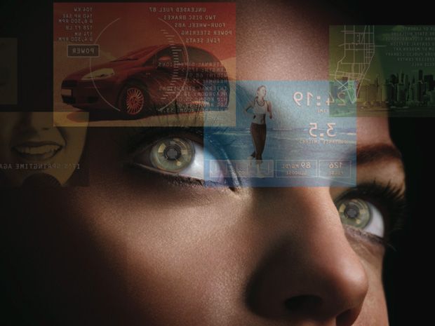
Image: Raygun Studio
The human eye is a perceptual powerhouse. It can see millions of colors, adjust easily to shifting light conditions, and transmit information to the brain at a rate exceeding that of a high-speed Internet connection.
But why stop there?
In the Terminator movies, Arnold Schwarzenegger’s character sees the world with data superimposed on his visual field—virtual captions that enhance the cyborg’s scan of a scene. In stories by the science fiction author Vernor Vinge, characters rely on electronic contact lenses, rather than smartphones or brain implants, for seamless access to information that appears right before their eyes.
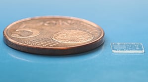
These visions (if I may) might seem far-fetched, but a contact lens with simple built-in electronics is already within reach; in fact, my students and I are already producing such devices in small numbers in my laboratory at the University of Washington, in Seattle [see sidebar, "A Twinkle in the Eye"]. These lenses don’t give us the vision of an eagle or the benefit of running subtitles on our surroundings yet. But we have built a lens with one LED, which we’ve powered wirelessly with RF. What we’ve done so far barely hints at what will soon be possible with this technology.
Conventional contact lenses are polymers formed in specific shapes to correct faulty vision. To turn such a lens into a functional system, we integrate control circuits, communication circuits, and miniature antennas into the lens using custom-built optoelectronic components. Those components will eventually include hundreds of LEDs, which will form images in front of the eye, such as words, charts, and photographs. Much of the hardware is semitransparent so that wearers can navigate their surroundings without crashing into them or becoming disoriented. In all likelihood, a separate, portable device will relay displayable information to the lens’s control circuit, which will operate the optoelectronics in the lens.
These lenses don’t need to be very complex to be useful. Even a lens with a single pixel could aid people with impaired hearing or be incorporated as an indicator into computer games. With more colors and resolution, the repertoire could be expanded to include displaying text, translating speech into captions in real time, or offering visual cues from a navigation system. With basic image processing and Internet access, a contact-lens display could unlock whole new worlds of visual information, unfettered by the constraints of a physical display.
Besides visual enhancement, noninvasive monitoring of the wearer’s biomarkers and health indicators could be a huge future market. We’ve built several simple sensors that can detect the concentration of a molecule, such as glucose. Sensors built onto lenses would let diabetic wearers keep tabs on blood-sugar levels without needing to prick a finger. The glucose detectors we’re evaluating now are a mere glimmer of what will be possible in the next 5 to 10 years. Contact lenses are worn daily by more than a hundred million people, and they are one of the only disposable, mass-market products that remain in contact, through fluids, with the interior of the body for an extended period of time. When you get a blood test, your doctor is probably measuring many of the same biomarkers that are found in the live cells on the surface of your eye—and in concentrations that correlate closely with the levels in your bloodstream. An appropriately configured contact lens could monitor cholesterol, sodium, and potassium levels, to name a few potential targets. Coupled with a wireless data transmitter, the lens could relay information to medics or nurses instantly, without needles or laboratory chemistry, and with a much lower chance of mix-ups.
Three fundamental challenges stand in the way of building a multipurpose contact lens. First, the processes for making many of the lens’s parts and subsystems are incompatible with one another and with the fragile polymer of the lens. To get around this problem, my colleagues and I make all our devices from scratch. To fabricate the components for silicon circuits and LEDs, we use high temperatures and corrosive chemicals, which means we can’t manufacture them directly onto a lens. That leads to the second challenge, which is that all the key components of the lens need to be miniaturized and integrated onto about 1.5 square centimeters of a flexible, transparent polymer. We haven’t fully solved that problem yet, but we have so far developed our own specialized assembly process, which enables us to integrate several different kinds of components onto a lens. Last but not least, the whole contraption needs to be completely safe for the eye. Take an LED, for example. Most red LEDs are made of aluminum gallium arsenide, which is toxic. So before an LED can go into the eye, it must be enveloped in a biocompatible substance.
So far, besides our glucose monitor, we’ve been able to batch-fabricate a few other nanoscale biosensors that respond to a target molecule with an electrical signal; we’ve also made several microscale components, including single-crystal silicon transistors, radio chips, antennas, diffusion resistors, LEDs, and silicon photodetectors. We’ve constructed all the micrometer-scale metal interconnects necessary to form a circuit on a contact lens. We’ve also shown that these microcomponents can be integrated through a self-assembly process onto other unconventional substrates, such as thin, flexible transparent plastics or glass. We’ve fabricated prototype lenses with an LED, a small radio chip, and an antenna, and we’ve transmitted energy to the lens wirelessly, lighting the LED. To demonstrate that the lenses can be safe, we encapsulated them in a biocompatible polymer and successfully tested them in trials with live rabbits.
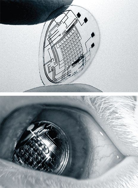
Photos: University of Washington Second Sight: In recent trials, rabbits wore lenses containing metal circuit structures for 20 minutes at a time with no adverse effects.
Seeing the light—LED light—is a reasonable accomplishment. But seeing something useful through the lens is clearly the ultimate goal. Fortunately, the human eye is an extremely sensitive photodetector. At high noon on a cloudless day, lots of light streams through your pupil, and the world appears bright indeed. But the eye doesn’t need all that optical power—it can perceive images with only a few microwatts of optical power passing through its lens. An LCD computer screen is similarly wasteful. It sends out a lot of photons, but only a small fraction of them enter your eye and hit the retina to form an image. But when the display is directly over your cornea, every photon generated by the display helps form the image.
The beauty of this approach is obvious: With the light coming from a lens on your pupil rather than from an external source, you need much less power to form an image. But how to get light from a lens? We’ve considered two basic approaches. One option is to build into the lens a display based on an array of LED pixels; we call this an active display. An alternative is to use passive pixels that merely modulate incoming light rather than producing their own. Basically, they construct an image by changing their color and transparency in reaction to a light source. (They’re similar to LCDs, in which tiny liquid-crystal ”shutters” block or transmit white light through a red, green, or blue filter.) For passive pixels on a functional contact lens, the light source would be the environment. The colors wouldn’t be as precise as with a white-backlit LCD, but the images could be quite sharp and finely resolved.
We’ve mainly pursued the active approach and have produced lenses that can accommodate an 8-by-8 array of LEDs. For now, active pixels are easier to attach to lenses. But using passive pixels would significantly reduce the contact’s overall power needs—if we can figure out how to make the pixels smaller, higher in contrast, and capable of reacting quickly to external signals.
By now you’re probably wondering how a person wearing one of our contact lenses would be able to focus on an image generated on the surface of the eye. After all, a normal and healthy eye cannot focus on objects that are fewer than 10 centimeters from the corneal surface. The LEDs by themselves merely produce a fuzzy splotch of color in the wearer’s field of vision. Somehow the image must be pushed away from the cornea. One way to do that is to employ an array of even smaller lenses placed on the surface of the contact lens. Arrays of such microlenses have been used in the past to focus lasers and, in photolithography, to draw patterns of light on a photoresist. On a contact lens, each pixel or small group of pixels would be assigned to a microlens placed between the eye and the pixels. Spacing a pixel and a microlens 360 micrometers apart would be enough to push back the virtual image and let the eye focus on it easily. To the wearer, the image would seem to hang in space about half a meter away, depending on the microlens.
Another way to make sharp images is to use a scanning microlaser or an array of microlasers. Laser beams diverge much less than LED light does, so they would produce a sharper image. A kind of actuated mirror would scan the beams from a red, a green, and a blue laser to generate an image. The resolution of the image would be limited primarily by the narrowness of the beams, and the lasers would obviously have to be extremely small, which would be a substantial challenge. However, using lasers would ensure that the image is in focus at all times and eliminate the need for microlenses.
Whether we use LEDs or lasers for our display, the area available for optoelectronics on the surface of the contact is really small: roughly 1.2 millimeters in diameter. The display must also be semitransparent, so that wearers can still see their surroundings. Those are tough but not impossible requirements. The LED chips we’ve built so far are 300 µm in diameter, and the light-emitting zone on each chip is a 60-µm-wide ring with a radius of 112 µm. We’re trying to reduce that by an order of magnitude. Our goal is an array of 3600 10-µm-wide pixels spaced 10 µm apart.
One other difficulty in putting a display on the eye is keeping it from moving around relative to the pupil. Normal contact lenses that correct for astigmatism are weighted on the bottom to maintain a specific orientation, give or take a few degrees. I figure the same technique could keep a display from tilting (unless the wearer blinked too often!).
Like all mobile electronics, these lenses must be powered by suitable sources, but among the options, none are particularly attractive. The space constraints are acute. For example, batteries are hard to miniaturize to this extent, require recharging, and raise the specter of, say, lithium ions floating around in the eye after an accident. A better strategy is gathering inertial power from the environment, by converting ambient vibrations into energy or by receiving solar or RF power. Most inertial power scavenging designs have unacceptably low power output, so we have focused on powering our lenses with solar or RF energy.
Let’s assume that 1 square centimeter of lens area is dedicated to power generation, and let’s say we devote the space to solar cells. Almost 300 microwatts of incoming power would be available indoors, with potentially much more available outdoors. At a conversion efficiency of 10 percent, these figures would translate to 30 µW of available electrical power, if all the subsystems of the contact lens were run indoors.
Collecting RF energy from a source in the user’s pocket would improve the numbers slightly. In this setup, the lens area would hold antennas rather than photovoltaic cells. The antennas’ output would be limited by the field strengths permitted at various frequencies. In the microwave bands between 1.5 gigahertz and 100 GHz, the exposure level considered safe for humans is 1 milliwatt per square centimeter. For our prototypes, we have fabricated the first generation of antennas that can transmit in the 900-megahertz to 6-GHz range, and we’re working on higher-efficiency versions. So from that one square centimeter of lens real estate, we should be able to extract at least 100 µW, depending on the efficiency of the antenna and the conversion circuit.
Having made all these subsystems work, the final challenge is making them all fit on the same tiny polymer disc. Recall the pieces that we need to cram onto a lens: metal microstructures to form antennas; compound semiconductors to make optoelectronic devices; advanced complementary metal-oxide-semiconductor silicon circuits for low-power control and RF telecommunication; microelectromechanical system (MEMS) transducers and resonators to tune the frequencies of the RF communication; and surface sensors that are reactive with the biochemical environment.
The semiconductor fabrication processes we’d typically use to make most of these components won’t work because they are both thermally and chemically incompatible with the flexible polymer substrate of the contact lens. To get around this problem, we independently fabricate most of the microcomponents on silicon-on-insulator wafers, and we fabricate the LEDs and some of the biosensors on other substrates. Each part has metal interconnects and is etched into a unique shape. The end yield is a collection of powder-fine parts that we then embed in the lens.
We start by preparing the substrate that will hold the microcomponents, a 100-µm-thick slice of polyethylene terephthalate. The substrate has photolithographically defined metal interconnect lines and binding sites. These binding sites are tiny wells, about 10 µm deep, where electrical connections will be made between components and the template. At the bottom of each well is a minuscule pool of a low-melting-point alloy that will later join together two interconnects in what amounts to micrometer-scale soldering.
We then submerge the plastic lens substrate in a liquid medium and flow the collection of microcomponents over it. The binding sites are cut to match the geometries of the individual parts so that a triangular component finds a triangular well, a circular part falls into a circular well, and so on. When a piece falls into its complementary well, a small metal pad on the surface of the component comes in contact with the alloy at the bottom of the well, causing a capillary force that lodges the component in place. After all the parts have found their slots, we drop the temperature to solidify the alloy. This step locks in the mechanical and electrical contact between the components, the interconnects, and the substrate.
The next step is to ensure that all the potentially harmful components that we’ve just assembled are completely safe and comfortable to wear. The lenses we’ve been developing resemble existing gas-permeable contacts with small patches of a slightly less breathable material that wraps around the electronic components. We’ve been encapsulating the functional parts with poly(methyl methacrylate), the polymer used to make earlier generations of contact lenses. Then there’s the question of the interaction of heat and light with the eye. Not only must the system’s power consumption be very low for the sake of the energy budget, it must also avoid generating enough heat to damage the eye, so the temperature must remain below 45 °C. We have yet to investigate this concern fully, but our preliminary analyses suggest that heat shouldn’t be a big problem.
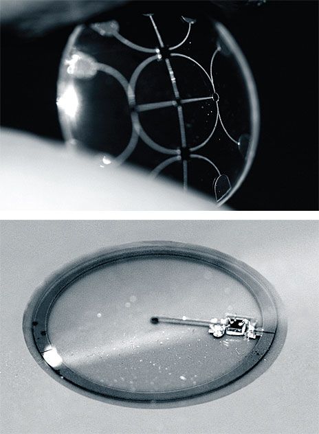
Photos: University of Washington In Focus: One lens prototype [left] has several interconnects, single-crystal silicon components, and compound-semiconductor components embedded within. Another sample lens [right] contains a radio chip, an antenna, and a red LED.
All the basic technologies needed to build functional contact lenses are in place. We’ve tested our first few prototypes on animals, proving that the platform can be safe. What we need to do now is show all the subsystems working together, shrink some of the components even more, and extend the RF power harvesting to higher efficiencies and to distances greater than the few centimeters we have now. We also need to build a companion device that would do all the necessary computing or image processing to truly prove that the system can form images on demand. We’re starting with a simple product, a contact lens with a single light source, and we aim to work up to more sophisticated lenses that can superimpose computer-generated high-resolution color graphics on a user’s real field of vision.
The true promise of this research is not just the actual system we end up making, whether it’s a display, a biosensor, or both. We already see a future in which the humble contact lens becomes a real platform, like the iPhone is today, with lots of developers contributing their ideas and inventions. As far as we’re concerned, the possibilities extend as far as the eye can see, and beyond.
The author would like to thank his past and present students and collaborators, especially Brian Otis, Desney Tan, and Tueng Shen, for their contributions to this research.
About the Author
Babak A. Parviz wakes up every morning and sticks a small piece of polymer in each eye. So it was only a matter of time before this bionanotechnology expert at the University of Washington, in Seattle, imagined contact lenses with built-in circuits and LEDs. “It’s really fun to hook things up and see how they might work,” he says. In “For Your Eye Only”, Parviz previews a contact lens for the 21st century.